| Content | | |
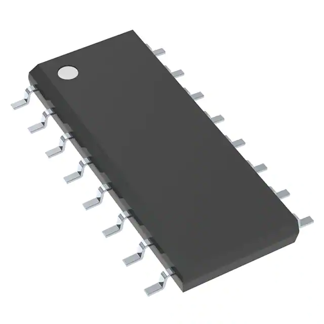
The PIC16F1503-I/P is an enhanced mid-range PIC16 family 8-bit powerful (200 nanosecond instruction execution) yet easy-to-program CMOS flash-based Microcontroller packs powerful PIC®(RISC) architecture. This product offers all of the advantages of the well-recognized mid-range x14 architecture with standardized features including 3.5kB of addressable program memory size, 128bytes of data memory size, 12 general-purpose I/O pins, two comparators, 8-channel 10-bit analog-to-digital (A/D) converter, and one 5-bit digital-to-analog (D/A) converter. This device operates at a maximum frequency of 20MHz with a wide operating voltage of 1.8 to 5.5V.
- 49 (14-bit wide) easy instructions to learn
- 16 level hardware stack
- 2 (16-bit) file select registers
- Hardware interrupt handling with the content save
- 16MHz internal oscillator
- Programmable brown-out reset (BOR)
- Power-on reset (POR)
- Internal voltage reference (Bandgap)
- Two 8-bit digital timers
- One 16-bit digital timer
- Four stand-alone PWM
- 2x Configurable logic cell modules (CLC)
- 1x Complementary waveform generator (CWG)/Complementary output generator (COG)
- Numerically controlled oscillator (NCO)
- In-Circuit Serial Programming (ICSP)
Applications
Industrial, Automotive, Consumer Electronics, Motor Drive & Control, Lighting, Medical, Security
Note:
- Product Images are shown for illustrative purposes only and may differ from the actual product.
- For Technical Specifications about the IC go through the Datasheet.
Package Includes:
1 x PIC 16F1503 20 MHz, 3.5 KB, 128 Byte 8-Bit MCU PIC16 Family Microcontroller IC
| |
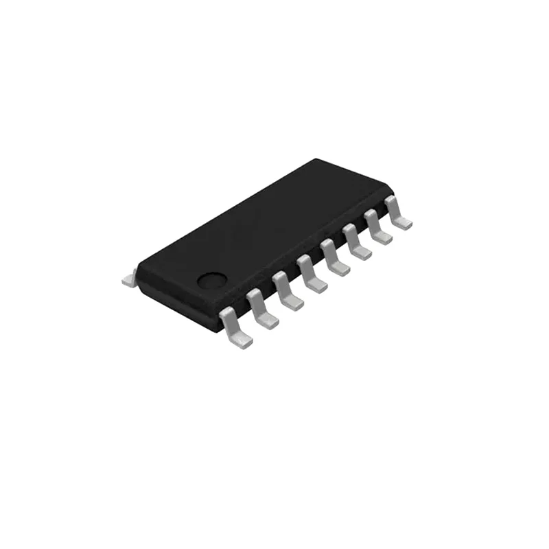
The NE555D is a precision timing circuits capable of producing accurate time delays or oscillation. In the time-delay or monostable mode of operation, the timed interval is controlled by a single external resistor and capacitor network. In the astable mode of operation, the frequency and duty cycle can be controlled independently with two external resistors and a single external capacitor. The threshold and trigger levels normally are two-thirds and one-third, respectively, of VCC. These levels can be altered by use of the control voltage terminal. When the trigger input falls below the trigger level, the flip-flop is set, and the output goes high. If the trigger input is above the trigger level and the threshold input is above the threshold level, the flip-flop is reset and the output is low.
Note: Image may vary from actual product in terms of Manufacturer/Brand name according to the availability.
Features:
- Timing from microseconds to hours
- A stable or monostable operation
- Adjustable duty cycle
- TTL compatible output can sink or source up to 200mA
- Applications: Clock & Timing, Consumer Electronics, Aerospace, Defence, Military, Embedded Design & Development
Package Includes:
1 x NE555DR SOIC-8 Timer (Pack of 5 ICs)
| Excellent chip to create multiple outputs from limited IO pins of microcontrollers.
The 74HC595; 74HCT595 is an 8-bit serial-in/serial or parallel-out shift register with a storage register and 3-state outputs. Both the shift and storage register have separate clocks. The device features a serial input (DS) and a serial output (Q7S) to enable cascading and an asynchronous reset MR input. A LOW on MR will reset the shift register. Data is shifted on the LOW-to-HIGH transitions of the SHCP input. The data in the shift register is transferred to the storage register on a LOW-to-HIGH transition of the STCP input. If both clocks are connected together, the shift register will always be one clock pulse ahead of the storage register. Data in the storage register appears at the output whenever the output enable input (OE) is LOW. A HIGH on OE causes the outputs to assume a high-impedance OFF-state. Operation of the OE input does not affect the state of the registers. Inputs include clamp diodes. This enables the use of current limiting resistors to interface inputs to voltages in excess of VCC. |