| Content | | |
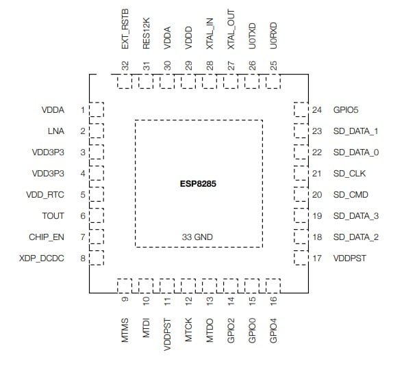
ESP8285 delivers highly integrated Wi-Fi SoC solutions to meet users’ continuous demands for efficient power usage, compact design and reliable performance in the Internet-of-Things industry. With the complete and self-contained Wi-Fi networking capabilities, ESP8285 can perform either as a standalone application or as the slave to a host MCU. When ESP8285 hosts the application, it promptly boots up from the flash. The integrated high-speed cache helps to increase system performance and optimize system memory. Also, ESP8285 can be applied to any microcontroller design as a Wi-Fi adaptor through SPI/SDIO or UART interfaces.
Pin Diagram
Features:
Package Includes:
1 x ESP8285 QFN32 IC Chip
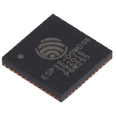
| ESP32 is a single 2.4 GHz Wi-Fi-and-Bluetooth combo chip designed with the TSMC ultra-low-power 40 nm technology. It is designed to achieve the best power and RF performance, versatility, and reliability in a wide variety of applications and power scenarios.
Ideal for low-power applications, the ESP32 SoC features fine-grained clock gating, multiple power modes, and dynamic power scaling. A low duty cycle is used to minimize the amount of energy that the ESP32 SoC expends. The output of the power amplifier is also adjustable, thus contributing to an optimal trade-off between communication range, data rate, and power consumption. The ESP32 SoC is highly-integrated with in-built antenna switches, power amplifiers, low-noise receive amplifiers, and power management modules. ESP32 adds priceless functionality and versatility to IoT applications with minimal Printed Circuit Board (PCB) requirements.
Pin Diagram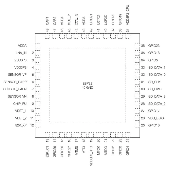
Features:
Package Includes:
1 x ESP32-D0WDQ6 IC QFN48 | Excellent chip to create multiple outputs from limited IO pins of microcontrollers.
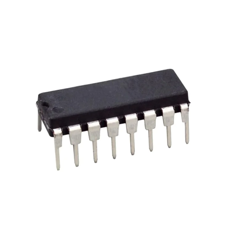
The 74HC595; 74HCT595 is an 8-bit serial-in/serial or parallel-out shift register with a storage register and 3-state outputs. Both the shift and storage register have separate clocks. The device features a serial input (DS) and a serial output (Q7S) to enable cascading and an asynchronous reset MR input. A LOW on MR will reset the shift register. Data is shifted on the LOW-to-HIGH transitions of the SHCP input. The data in the shift register is transferred to the storage register on a LOW-to-HIGH transition of the STCP input. If both clocks are connected together, the shift register will always be one clock pulse ahead of the storage register. Data in the storage register appears at the output whenever the output enable input (OE) is LOW. A HIGH on OE causes the outputs to assume a high-impedance OFF-state. Operation of the OE input does not affect the state of the registers. Inputs include clamp diodes. This enables the use of current limiting resistors to interface inputs to voltages in excess of VCC. | |